DMON SOC support
ARM support
DMON v2 integrates the Segger J Link debug link and adds proof of concept support for a single ARM target - STM32L152VB. The Segger J Link supports a huge number of processors, see https://www.segger.com/jlink_supported_devices.html . DMON2 customers can request support for additional ARM devices.
The following command line options must be passed to DMON for this mode:
- -arm Start DMON in ARM mode and load ARM specific commands
- -segger Use Segger J-Link
- -device STM32L152VB specify the device for Segger
- -swd Use the Serial Wire Debug interface (SWD). If not specified then Segger will use JTAG to communicate with the target. The use of SWD is optional but recommended.
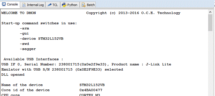
When DMON is started with the appropriate ARM switches information about the link discovered is displayed (as below).
The device configuration for the ARM target is read from an ARM CSMIS SVD file which describes the peripheral devices and their registers. In this version this SVD file is included as part of the built DMON and only this file is loaded and used. The output below shows device and peripheral information.
Name of the device                STM32L152VB
Core id of the device             0x4BA00477
CPU core                          CORTEX_M3
Device manufacturer               ST
Start address of flash area       0x08000000
Start address of RAM area         0x20000000
0=Little, 1=Big, 2=Both           0
Total flash size in bytes         132 KB
Total RAM size in bytes           16 KB
Flash regions :
  Start Address:                  0x08000000
  Size:                           128 KB
  Start Address:                  0x08080000
  Size:                           4 KB
RAM regions :
  Start Address :                 0x20000000
  Size :                          16 KB

OEM : IAR
Target Voltage = 3.338 V

Connected with SWD

Identified ::: Cortex-M3 core
Target interface speed: 1000 kHz
Peripheral Devices:
C_ADC     Common ADC registers                                        N/A
COMP      Comparators                                                 N/A
CRC       CRC calculation unit                                        N/A
DAC       Digital-to-analog converter                                 N/A
DMA1      Direct memory access controller                             N/A
EXTI      External interrupt/event controller                         N/A
Flash     Flash                                                       N/A
GPIOA     General-purpose I/Os                                        N/A
GPIOB     General-purpose I/Os                                        N/A
GPIOC     General-purpose I/Os                                        N/A
GPIOD     General-purpose I/Os                                        N/A
GPIOE     General-purpose I/Os                                        N/A
GPIOH     General-purpose I/Os                                        N/A
I2C1      Inter-integrated circuit                                    N/A
I2C2      Inter-integrated circuit                                    N/A
IWDG      Independent watchdog                                        N/A
LCD       Liquid crystal display controller                           N/A
PWR       Power control                                               N/A
RCC       Reset and clock control                                     N/A
RI        Routing interface                                           N/A
RTC       Real-time clock                                             N/A
SPI1      Serial peripheral interface                                 N/A
SPI2      Serial peripheral interface                                 N/A
SYSCFG    System configuration controller                             N/A
TIM10     General-purpose timers                                      N/A
TIM11     General-purpose timers                                      N/A
TIM2      General-purpose timers                                      N/A
TIM3      General-purpose timers                                      N/A
TIM4      General-purpose timers                                      N/A
TIM6      Basic timers                                                N/A
TIM7      Basic timers                                                N/A
TIM9      General-purpose timers                                      N/A
USART1    Universal synchronous asynchronous receiver transmitter     N/A
USART2    Universal synchronous asynchronous receiver transmitter     N/A
USART3    Universal synchronous asynchronous receiver transmitter     N/A
USB       Universal serial bus full-speed device interface            N/A
USB_SRAM  Universal serial bus full-speed device interface            N/A
WWDG      Window watchdog                                             N/A
ADC       Analog-to-digital converter                                 N/A
NVIC      Nested Vectored Interrupt Controller                        N/A
DBG       Debug support                                               N/A
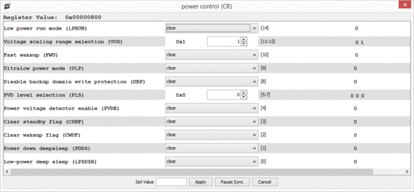
The SVD is used create objects for each peripheral device, to build a layout diagram for the SoC with the same functionality as for SPARC devices, and a widget with a drop down list of the registers for each peripheral.
There is also an object and widget for the CPU (see below).
On-chip IP blocks can be selected and their registers viewed and modified through the GUI.
ARM supported DMON commands
When in ARM mode the console supports the following commands:
| Command | Description |
|---|---|
| about | display information about DMON version |
| breakh <addr|symbol> | display breakpoints or add hardware breakpoint |
| breaks <addr|symbol> | display or add software breakpoint |
| clear <num|address> | delete all breakpoints or breakpoint at number or address |
| cls | clear console |
| code <addr|PC> <length> <mode> | Disassemble <length> instructions starting at <address> or current PC using <mode> (ARM or Thumb).Default mode is the currently set mode, this will normally correctly recognise whether the instruction is ARM or Thumb. |
| continue | continue execution |
| datamon load [filename] | load a DataSet from an xml file |
| datamon save [filename] | save the current DataSet to an xml file |
| datamon start | Validate the current DataSet if successful, start monitoring |
| datamon stop | stop monitoring |
| datamon xsd [filename] | save schema for DataSet to the specified file |
| devreg | list available devices |
| devreg <name> | display registers in <name> |
| devreg <name> <regname> | display register detail for <regname> in <name> |
| devreg <name> <regname> <value> | Write <value> to <regname> in <name> |
| devreg <name> list | list register names in <name> |
| dmon | Use only DMON commands. Ignored if already in DMON mode |
| echo [string] | display string in the console (and log file if active) |
| examine [addr] <length> | display memory |
| exec [command] | execute shell command in OS |
| flash erase | erase flash device |
| font | show current font |
| font list | list system fonts |
| font reset | reset the font to the default |
| font set [value] | set font |
| gb2312 | Use GB2312 character set for displaying memory data |
| getb [address] <count> | Returns a byte or array of <count> bytes in the command response (for scripting in Tcl) |
| getstate | returns 1 if an application is running on the target, 0 otherwise. (for scripting in Tcl) |
| getw [address] <count> | Returns a word or array of <count> words in the command response |
| halt | stop program on board |
| help <command> | display commands or command |
| info dev | list devices available for info dev command |
| info dev <name> | display information for device <name> |
| info sys | display basic system information |
| log [file_name] | open log file or create new and output some system information |
| loglevel [level] | set internal logging to level. Possible levels [verbose|restore|info|warn|error] |
| logoff | stop output to file |
| lookup [hex value] | show the ELF symbol matching the hex address |
| lookup [symbol or expression] | show the value of the symbol (internal or ELF) |
| pause -1 | pause script until processor stops |
| pause [duration in ms] | pause script until duration has elapsed or processor stops |
| precont [filename] | append a script to the user scripts executed before continuing/stepping a program |
| precont insert [index] [filename] | insert a script at [index] in the user scripts executed before continuing/stepping a program |
| precont list | list the user scripts executed before continuing/stepping a program |
| precont remove [index|all] | remove the script at [index] in the user scripts or all scripts executed before continuing/stepping a program |
| prerun [filename] | append a script to the user scripts executed before starting a program |
| prerun insert [index] [filename] | insert a script at [index] in the user scripts executed before starting a program |
| prerun list | list the user scripts executed before starting a program |
| prerun remove [index|all] | remove the script at [index] in the user scripts or all scripts executed before starting a program |
| printreg | display system registers |
| python | Interpret command input as Python commands. Ignored if in Python mode |
| quit | exit DMON |
| reg | show values for all available CPU registers |
| reg <name> | show register named |
| reg <name> <value> | write value to register named |
| reg show | show available register names |
| run <pc> | start the CPU from <pc> |
| runscript [filename] | set the user script executed during program execution |
| runscript list | list the user script executed during program execution |
| runscript remove | clear the user script executed during program execution |
| save [addr] [addr] [file] <bin> | dump target memory to file in srecord (or binary) format |
| script [file_name] | execute a batch file of DMON commands |
| setv [label] [expression] | Sets a DMON label to have a 64 bit integer value |
| shell | In a startup script activate the language specified by command line option. Otherwise, display the langauge in use. |
| step <n> | single step one or <n> times |
| stop | Invoked on CTRL-C. Abort DMON command,stop program on board |
| symbols <file> | show/load symbols |
| tcl | Interpret command input as Tcl commands. Ignored if in Tcl mode |
| utf8 | Use UTF-8 character set for displaying memory and UART data |
| watch <addr|symbol> | display all breakpoint or add data watchpoint on read or write |
| watchr <addr|symbol> | display all breakpoint or add data watchpoint on read |
| watchw <addr|symbol> | display all breakpoint or add data watchpoint on write |
| write [addr] [data] <number words> | write one word of data to "number words" starting from addr |
ARM specific commands
The devreg commands are specific to ARM peripherals, and display or modify the registers in a specified peripheral:
DMON > devreg

Available devices:
ADC            COMP           CRC            C_ADC
DAC            DBG            DMA1           EXTI
FLASH          GPIOA          GPIOB          GPIOC
GPIOD          GPIOE          GPIOH          I2C1
I2C2           IWDG           LCD            NVIC
PWR            RCC            RI             RTC
SPI1           SPI2           SYSCFG         TIM10
TIM11          TIM2           TIM3           TIM4
TIM6           TIM7           TIM9           USART1
USART2         USART3         USB            USB_SRAM
WWDG

DMON > devreg gpioe

GPIOE
 0x40021000   GPIO port mode (MODER)                   0x00500000
 0x40021004   GPIO port output type (OTYPER)           0x00000000
 0x40021008   GPIO port output speed (OSPEEDER)        0x00f00000
 0x4002100c   GPIO port pull-up/pull-down (PUPDR)      0x00000000
 0x40021010   GPIO port input data (IDR)               0x00001000
 0x40021014   GPIO port output data (ODR)              0x00000000
 0x40021018   GPIO port bit set/reset (BSRR)           0x00000000
 0x4002101c   GPIO port configuration lock (LCKR)      0x00000000
 0x40021020   AFRL (AFRL)                              0x00000000
 0x40021024   GPIO alternate function high (AFRH)      0x00000000

DMON > devreg gpioe odr 0xffffffff

Wrote value 0xffffffff to odr

DMON > devreg gpioe

GPIOE
 0x40021000   GPIO port mode (MODER)                   0x00500000
 0x40021004   GPIO port output type (OTYPER)           0x00000000
 0x40021008   GPIO port output speed (OSPEEDER)        0x00f00000
 0x4002100c   GPIO port pull-up/pull-down (PUPDR)      0x00000000
 0x40021010   GPIO port input data (IDR)               0x00001c00
 0x40021014   GPIO port output data (ODR)              0x0000ffff
 0x40021018   GPIO port bit set/reset (BSRR)           0x00000000
 0x4002101c   GPIO port configuration lock (LCKR)      0x00000000
 0x40021020   AFRL (AFRL)                              0x00000000
 0x40021024   GPIO alternate function high (AFRH)      0x00000000
AGGA-4 Support
AGGA-4 hardware
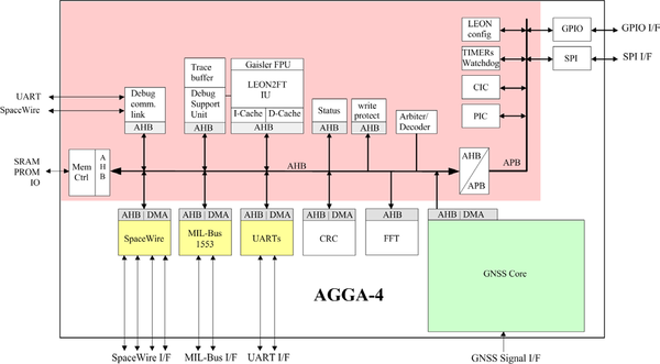
The AGGA-4 (Advanced GPS/GALILEO ASIC) is a radiation tolerant GNSS baseband ASIC capable of processing the modernized GPS and Galileo Signals. Due to its flexibility it is also able to process not only GPS and Galileo but also other GNSS systems like Glonass, Compass, etc. AGGA-4 also incorporates the processor, the communication interfaces and other support functions (e.g. FFT, CRC) inside the ASIC which simplifies the GNSS receiver board design.
The functional blocks are shown in the diagram below.
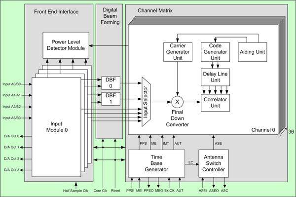
The GNSS Core (shown below) consists of 4 Input Modules (IM), one Power Level Detector (PLD) Module, two Beam Forming (DBF) Modules, a Time Base Generator (TBG), an Antenna Switch Controller (ASC) and 36 channels.
DMON supports the functional blocks on the AGGA-4 and the specific features below:
- System Visualisation
- Devices present and their state
- Register details/modify
- GNSS
- Configuration Blocks Display and Modify
- Interrupt Configuration
- Power Level
- Channel Configurations
- Overall display
- Set, Copy, Modify, Save and Load
- Dump observables to file
- FFT
- CRC
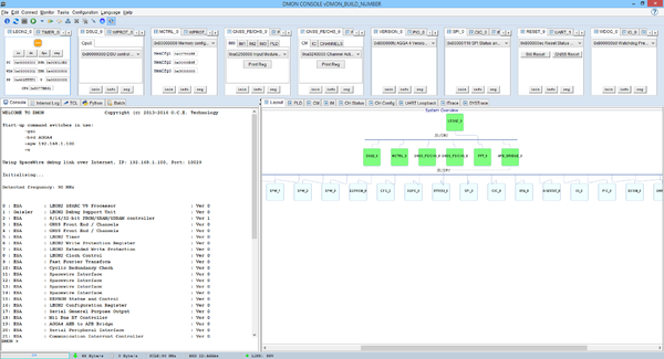
See below some example screenshots from the tool.
Main AGGA4 console
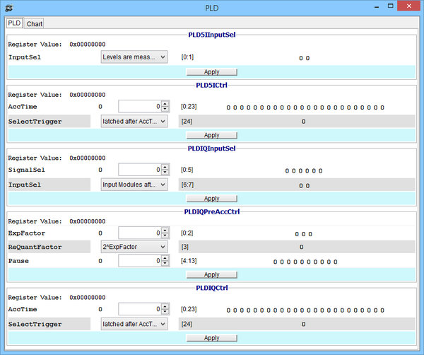
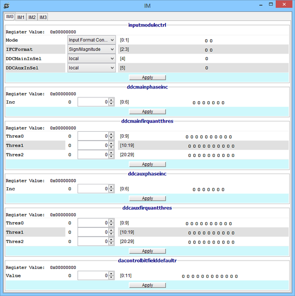
GNSS on AGGA4 has a lot of Configuration Registers. DMON identifies GNSS as AGGA4_GNSS_FE/CHS dummy device and logically AGGA4_GNSS_FR_END device (IM0, IM1, IM2, IM3 and PLD) and AGGA4_GNSS_CHS device (Channel Matrix, IC, Channels).
Power Level Detector window
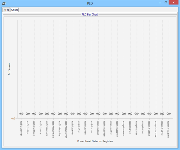
Power Level Detector chart
DMON reads PLD Accumulation Registers and Displays as Bar Chart
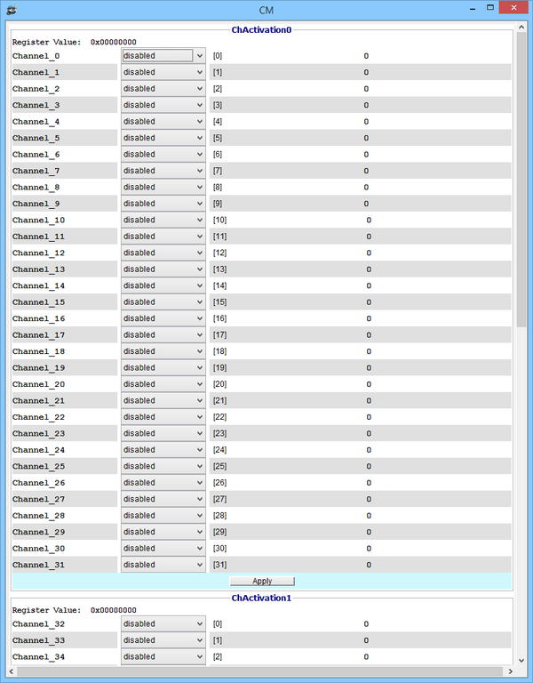
Channel Matrix Window
Input Module window
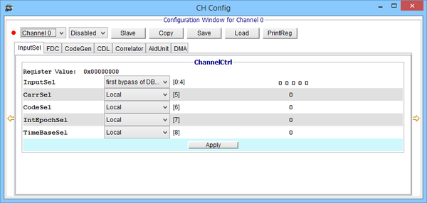
Channel Control window
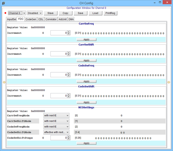
Channel Final Down Converter window
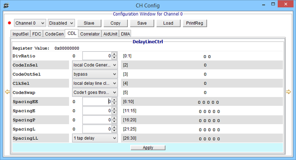
Channel Code Delay Line Unit window
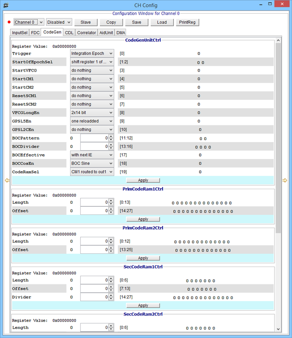
Channel Code Generator Unit window
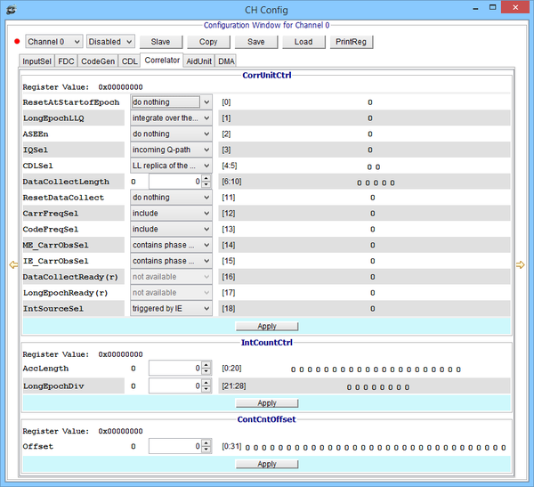
Channel Correlator Unit window
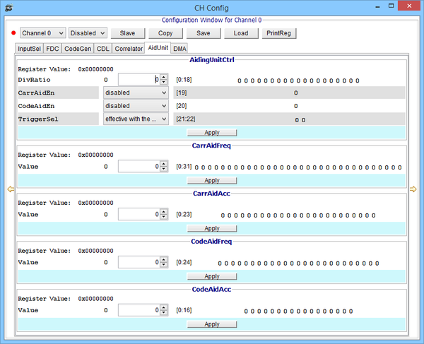
Channel Aiding Unit window
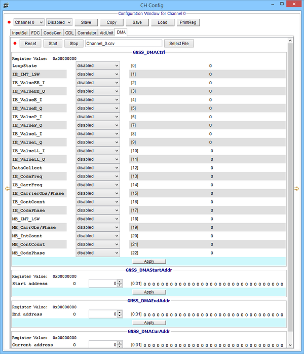
Channel GNSS DMA window
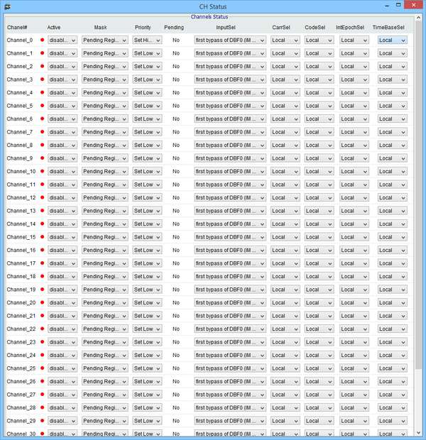
Channel Status window
Commands
The sections below describe the AGGA-4 commands. The table below is a summary of these commands.
| Command | Description |
|---|---|
| gnss copy <nomem>[ch[#]..ch[n]/all] | copy config from ch# to other space separated channels/all if <nomem> used the RAM code not copied |
| gnss [save/load] ch# file | Save/load Channel Configurations to File as xml |
| gnss dump [start/stop] ch# file | Start/Stop dumping of Channel Observables to File |
| gnss dump reset ch# | Reset dumping of Channel Observables to initial state |
| gnss printreg ch [#] [RegName] | Display Registers/Register for GNSS Channel [number] |
| gnss printreg cm [RegName] | Display Registers/Register for GNSS Channel Matrix |
| gnss printreg ic [RegName] | Display Registers/Register for GNSS Interrupt Controller |
| gnss printreg im [#][RegName] | Display Registers/Register for GNSS Input Module |
| gnss printreg pld [RegName] | Display Registers/Register for GNSS POWER LEVEL DETECTOR |
| gnss setreg ch [#] [RegName/FieldName][val] | Set Register/Bitfield for GNSS Channel [number] |
| gnss setreg cm [RegName/FieldName][val] | Set Register/Bitfield for GNSS Channel Matrix |
| gnss setreg ic [RegName/FieldName][val] | Set Register/Bitfield for GNSS Interrupt Controller |
| gnss setreg im [#][RegName/FieldName][val] | Set Register/Bitfield for GNSS Input Module |
| gnss setreg pld [RegName/FieldName][val] | Set Register/Bitfield for GNSS PLD |
| gnss slave [ch[#] ch[n]/all] | Slave channel/channels from to/all to previous Channel |
| fft <display> | Periodically checks FFT_Done bit and display results, <display> opens up graph panel |
| fft [file in] <optional> | Processes input file in pairs of 128, if output file is omitted then results will be stored .out.csv added to end of [file in]. Possible optional arguments are <file out> <nohex,onlyhex> |
| fft stop | Stops periodically polling |
| crc alias [name][poly][init] <opt> | Creates new alias, option arguments are <xor> <revdata> <revrslt> |
| crc alias display | Display list of aliases in current DMON session |
| crc calculate [bin] <addr> | Calculates crc of bin file, addr argument sets starting address for file |
| crc calculate [elffile] <sections> | Calculates crc of elf file, section argument allows calculation only on that section |
| crc calculate [srec] | Calculates crc of srec file |
| crc calculate [start][end]<init> | Calculates crc of a range of address, if init value is specified then that value will be written to CRCLFSR register before beginning. |
| crc init [alias] | Initialises CRC device with values in alias |
| crc init [ploy][init] <opt> | Initialises CRC device, optional arguments are <xor> <revdata> <revrslt> |
| reset <software/gnss> | Reset system software or gnss software |
| reset set <key> <value> | set the reset key <swen, swex, gnssen, gnssex> with value |
| spwdebug <IP/port> <port> | Change debug link to SpaceWire port |
GNSS commands
DMON > gnss copy nomem ch0 ch1
Configurations from Channel 0 were copied to Channel 1 without RAM DATA
DMON > gnss copy ch0 ch1 ch2
Configurations from Channel 0 were copied to Channel 1
Configurations from Channel 0 were copied to Channel 2
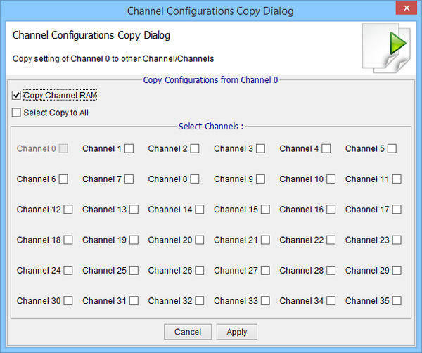
Or Alternatively Copy Dialog Window can be used
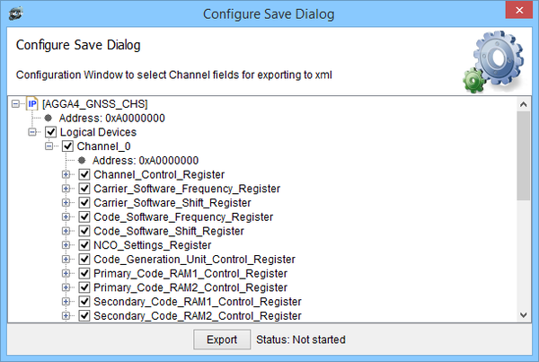
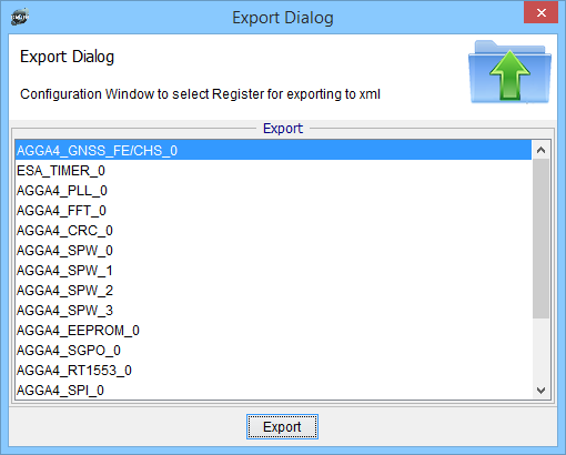
The user can select Channel, Configuration Registers and Values for exporting to xml file. This file can be loaded later for the same Channel or any other.
DMON > gnss save ch0 MyFile.xml
Currently processing XML, please wait
Successfully save configuration to C:\Projects\OCE\trunk\dmon_product\com.oce.dmon\MyFile.xml
DMON > gnss load ch0 MyFile.xml
Processing XML
Initialising Registers
Successfully initialised registers
Dialog to Save Channel configurations to xml file below.
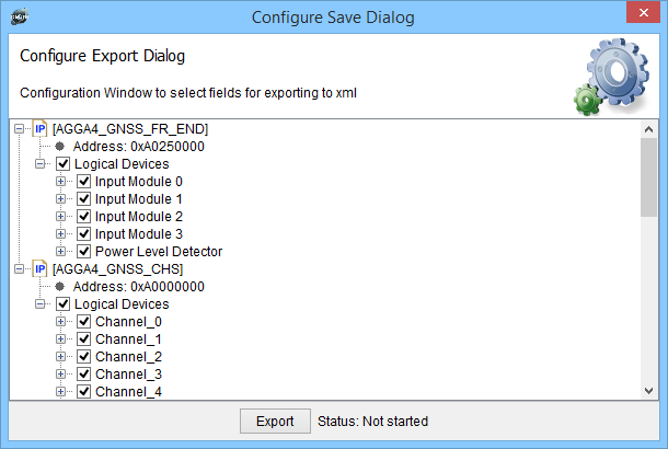
Dialog to Save GNSS to xml file below.
Dialog to Save AGGA4 specific registers to xml file below.
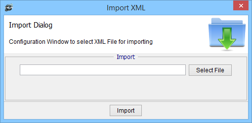
Dialog to select xml configuration file to be imported below.
DMON > gnss printreg ch 0
AGGA4 GNSS CHANNEL 0 Registers
 0xa0000000   channelctrl                              0x00000000
 0xa0000004   carrswfreq                               0x00000000
 0xa0000008   carrswshift                              0x00000000
 0xa000000c   codeswfreq            ….
DMON > gnss printreg ch 0 channelctrl
GNSS Channel #0 Reg :: channelctrl =  0x00000000
Register Contents                       : 0x00000000
[ 0, 4]:InputSel                              : first bypass of DBF0 (IM 0)
   [ 5]:CarrSel                                : Local
   [ 6]:CodeSel                                : Local
   [ 7]:IntEpochSel                         : Local
   [ 8]:TimeBaseSel                        : Local
DMON > gnss printreg cm
AGGA4 GNSS CHANNEL MATRIX  Registers :
 0xa0240000   chactivation0                            0x00000001
 0xa0240004   chactivation1                            0x00000000
 0xa0240008   dbfinputsel                              0x00000000
 0xa024000c   epochclkdiv       …
DMON > gnss printreg cm  chactivation0

GNSS Channel Matrix Reg :: chactivation0 =  0x00000001
Register Contents                       : 0x00000001
   [ 0]:Channel_0                              : enabled
   [ 1]:Channel_1                              : disabled
   [ 2]:Channel_2                              : disabled
   [ 3]:Channel_3                              : disabled
   [ 4]:Channel_4                              : disabled
   [ 5]:Channel_5                              : disabled
   [ 6]:Channel_6   ….
DMON > gnss printreg ic

AGGA4 GNSS Interrupt Controller Registers :
 0xa02c0000   gic_mask0                            0x00000000
 0xa02c0004   gic_mask1                            0x00000000
 0xa02c0008   gic_prio0                            0x00000001
 0xa02c000c   gic_prio1                            0x00000000
 0xa02c0010   gic_pend0                            0x00000000
 0xa02c0014   gic_pend1                            0x00000070
 0xa02c0018   gic_clear0                           0x00000000
 0xa02c001c   gic_clear1                           0x00000000
 0xa02c0020   gic_queuelow                         0x0000003f
 0xa02c0024   gic_queuehigh                        0x0000003f
 0xa02c0028   gic_queuestatus                      0x00000000
DMON > gnss printreg ic  gic_mask0

GNSS Interrupt Controller Reg :: gic_mask0 =  0x00000000
Register Contents                       : 0x00000000
   [ 0]:Channel_0                              : Pending Register
   [ 1]:Channel_1                              : Pending Register
   [ 2]:Channel_2                              : Pending Register
   [ 3]:Channel_3                              : Pending Register
   [ 4]:Channel_4                              : Pending Register
   [ 5]:Channel_5    …
DMON > gnss printreg im 0

AGGA4 GNSS Input Module_0 Registers :
 0xa0250000   inputmodulectrl                          0x00000000
 0xa0250004   ddcmainphaseinc                          0x00000000
 0xa0250008   ddcmainfirquantthres                     0x00000000
 0xa025000c   ddcauxphaseinc                           0x00000000
 0xa0250010   ddcauxfirquantthres                      0x00000000
 0xa0250014   dacontrolbitfielddefaultr                0x00000000
DMON > gnss printreg im 0  inputmodulectrl

GNSS Input Module #0 Reg :: inputmodulectrl =  0x00000000
Register Contents                       : 0x00000000
[ 0, 1]:Mode                                   : Input Format Converter Mode (IFC)
[ 2, 3]:IFCFormat                              : Sign/Magnitude
   [ 4]:DDCMainInSel                           : local
   [ 5]:DDCAuxInSel                            : local
DMON > gnss printreg pld

AGGA4 GNSS POWER LEVEL DETECTOR Registers :
 0xa02b0000   pld5iinputsel                            0x00000000
 0xa02b0004   pld5ictrl                                0x00000000
 0xa02b0008   pldiqinputsel                            0x00000000
 0xa02b000c   pldiqpreaccctrl                          0x00000000
 0xa02b0010   pldiqctrl                                0x00000000
 0xa02b0014   acc5iplusseven                           0x00000000
 0xa02b0018   acc5iplusfive                            0x00000000
 0xa02b001c   acc5iplusthree      …
DMON > gnss printreg pld pld5ictrl
GNSS Power Level Detector Reg :: pld5ictrl =  0x00000000
Register Contents                       : 0x00000000
[ 0,23]:AccTime                                : 0
   [24]:SelectTrigger                          : latched after AccTime Samples
DMON > gnss setreg cm chactivation0 0xffffffff

Value for Register chactivation0 set to 0xFFFFFFFF
DMON > gnss setreg cm chactivation0 Channel_0  0x0

Value for Register chactivation0 set to 0xFFFFFFFE
DMON > gnss slave ch1

Channel 1 was set as Slave
FFT commands
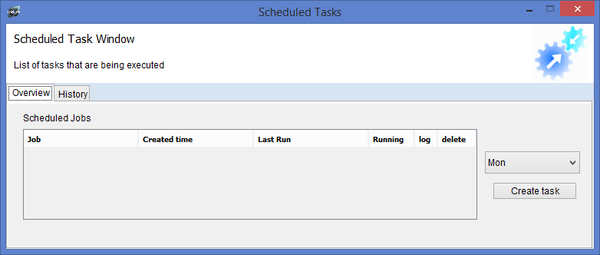
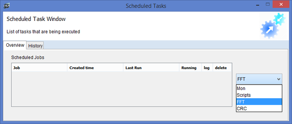
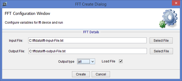
Creating FFT Task through the gui, start by clicking on the menu Tasks>>Configure Tasks.
Find FFT and click create task.
If you don’t enter an output file, then an output file will be generated in the input file directory with the same filename but suffixed with .csv.
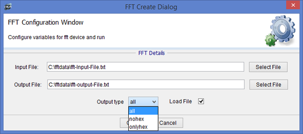
The output type can be changed to have all (which includes the hex and float values) or just hex or float. All is set by default.
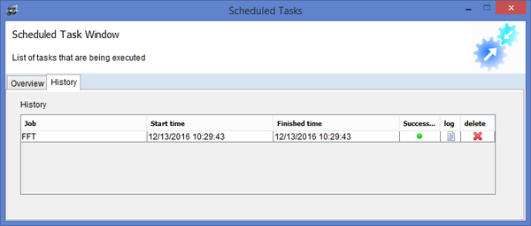
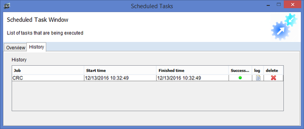
When the job is running, it will be located in the overview window, when it is done, it will be moved to the history tab. You will be able to see the time it took for the task to run as well as the result. You can click on the log icon to open the log window or alternatively clicking on the x icon deletes the task from history.
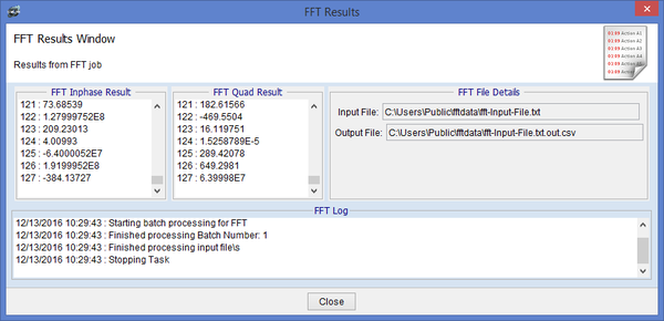
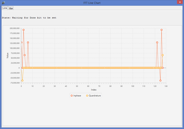
Here is the results from the FFT task, as you can see a csv suffix was added to the output file. As well as the results being displayed in the Inphase and Quad phase Panels you will also notice log information for this task.
You can also view the fft information via a line or bar graph by issuing the fft display command.
COMMANDS
fft <display> Periodically checks FFT_Done bit and display results, <display> opens up graph panel
DMON  > fft

Waiting for Done bit to be set
fft [file in] <optional> Processes input file in pairs of 128, if output file is omitted then results will be stored .out.csv added to end of [file in]. Possible optional arguments are <file out> <nohex|onlyhex>
DMON > fft C: /newline_sep_data_full.txt    C: /newline_data_full_output.txt

Starting batch processing for FFT
Finished processing Batch Number: 1
Finished processing input file\s
DMON > fft C: /newline_sep_data_full.txt    C: /newline_data_full_output.txt onlyhex
Starting batch processing for FFT
Finished processing Batch Number: 1
Finished processing input file\s
DMON > fft C: /newline_sep_data_full.txt    C: /newline_data_full_output.txt nohex
Starting batch processing for FFT
Finished processing Batch Number: 1
Finished processing input file\s
DMON > fft C: /newline_sep_data_fIll.txt    C: /newline_data_fill_output.txt
Starting batch processing for FFT
Finished processing Batch Number: 1
Finished processing Batch Number: 2
Finished processing input file\s
fft stop Stops periodically polling
DMON > fft stop
Stopped FFT batch processing
CRC commands
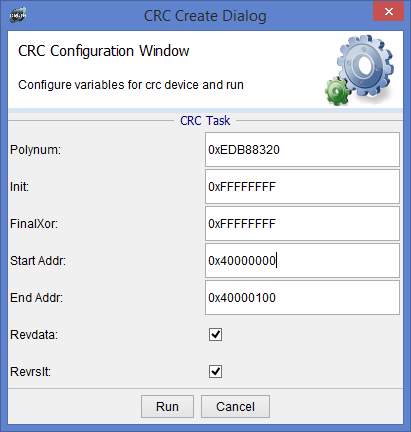
You can create a CRC task by clicking on CRC in the dropdown menu and clicking create task. Here you will be able to set the different properties to be used for generating the CRC.
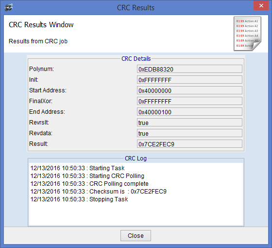
The results window shows what properties you used to generate the CRC as well as the result and log of the crc task.
COMMANDS
crc alias [name][poly][init] <opt> Creates new alias, option arguments are <xor> <revdata> <revrslt>
DMON > crc alias myAlias 0x3 0x4 0x5 1 1
Successfully added myAlias alias
crc alias display Display list of aliases in current DMON session
DMON > crc alias display
Name	Polynum		Init		FinalXOR	RevIn	RevRes
crc16	0x0000A001	0x00000000	0x00000000	true	true
ccitt	0x00008408	0x0000FFFF	0x00000000	false	false
crc32	0xEDB88320	0xFFFFFFFF	0xFFFFFFFF	true	true
myAlias	0x00000003	0x00000004	0x00000005	true	true
crc calculate [bin] <addr> Calculates crc of bin file, addr argument sets starting address for file
DMON > crc calculate C: /binaryfileAGGA4.bin 0x40000024
Binary File
Loading file from address: 0x40000024
Wrote bytes        0%
Entry point: 0x40000024

There are no Sections in this file. Calculating CRC for Loaded file

Starting CRC Polling
CRC Polling complete
Checksum is  : 0xDCC7C62F
GR716 Support
GR716 Microcontroller
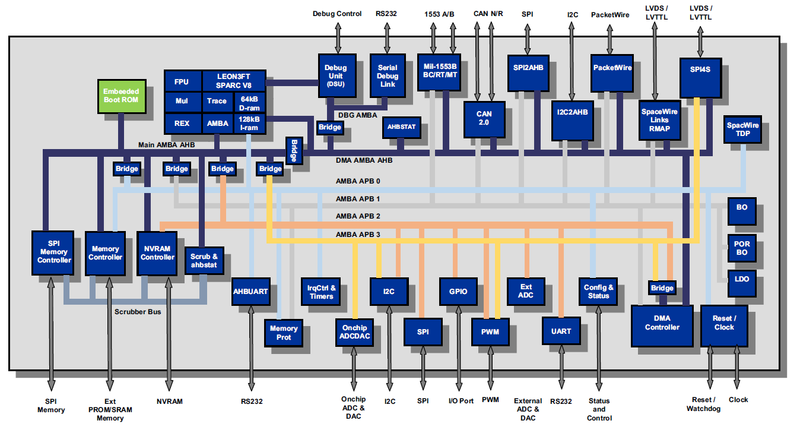
DMON supports the GR716 microcontroller from Cobham-Gaisler. This microcontroller features a fault-tolerant LEON3 SPARC V8 processor, communication interfaces and on-chip ADC, DAC, Power-on-Reset, Oscillator, Brown-out detection, LVDS transceivers, regulators to support for single 3.3V supply, ideally suited for space and other high-rel applications. A block diagram of the GR716 is shown below. DMON provides support for all the functional units on the microcontroller. The sections below provide more information on DMON support for some specific functional units of the microcontroller.
Credit: GR716 User Manual Version 1.26
Startup Options
The table below shows GR716 startup options.
| Command | Description |
|---|---|
| -iomx set [configName configName ...] | Set IOMX configurations for Device or Array of Devices (see IO switch matrix section below) |
| -grcg or grcg_(index) [enable|disable][all|bit..bitN] | Enable|Disable all, single bit or array of bits for GRCLKGATE_(DeviceIndex) (see clock gating section below) |
Typical startup options used with the GR716 Mini development board are
-gui
-u
-baud 230400
-iomx set mem_gr716_mini_cfg0
-grcg enable 0x4 16
-nosram_1
Layout window
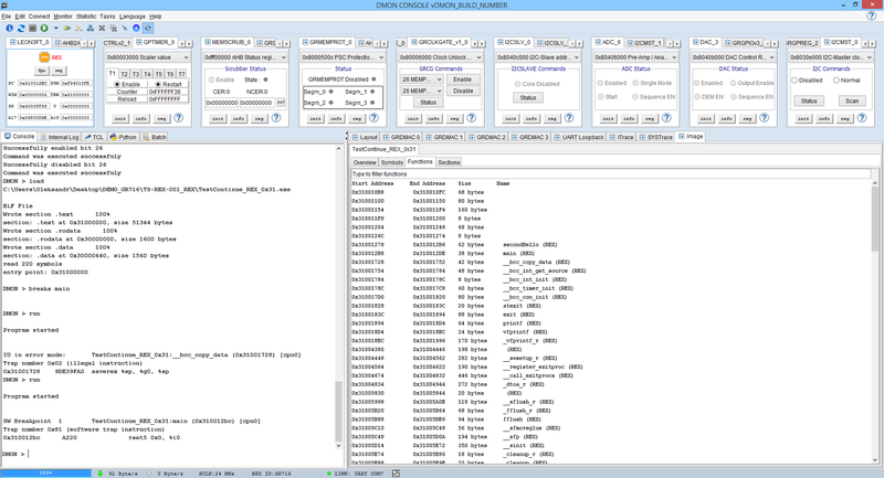
DMON represents the GR716 SOC in the layout below. By clicking on a functional block it's IP and register definitions are displayed in separate windows.
REX support
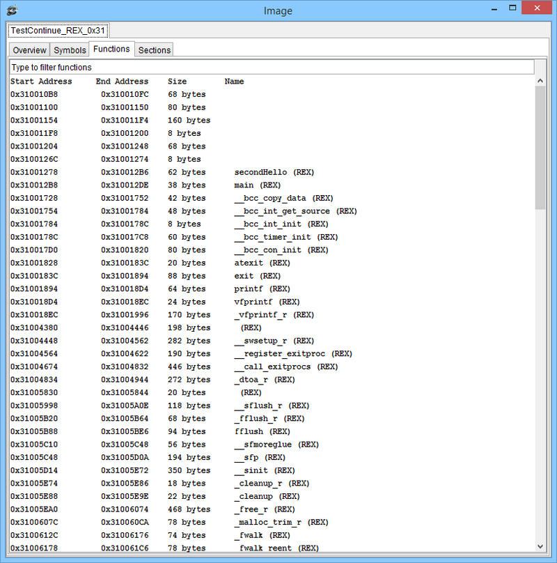
DMON supports the 16 bit REX instruction set.
DMON Functions View of loaded image (REX functions are marked with (REX))
Instruction Trace Information
DMON > inst 40

Rex    Time      Address   Instruction                                    Result
R   00000008763  3100A170  ld [%i2 + 0x8], %l6 (rld [%i2 + 0x8], %l6)     [0000000C]
R   00000008765  3100A174  sub %l6, %i0, %l6 (rsub %i0, %l6)              [00000000]
R   00000008766  3100A176  cmp %l6, 0x0 (rcmp %l6, 0x0)                   [00000000]
R   00000008767  3100A178  add %i5, %i0, %i5 (radd %i0, %i5)              [3000005A]
R   00000008768  3100A17A  sub %i4, %i0, %i4 (rsub %i0, %i4)              [00000000]
R   00000008770  3100A17C  st %l6, [%i2 + 0x8] (rst %l6, [%i2 + 0x8])     [3000FEB0][00000000]
R   00000008771  3100A180  bne TestContinue_REX_0x31:__sfvwrite_r + 0x238 (rbne 0xffffff32)  [00000000]
R   00000008772  3100A182  add %g0, 0x0, %i0 (rset5 0x0, %i0)             [00000000]
R   00000008773  3100A184  ret (rretrest)                                 [3100A181]
R   00000008774  3100A184  restore %i7, 0x8, %g0 (rretrest)               [31007E07]
R   00000008777  31007E06  add %g0, %o0, %i0 (rmov %o0, %i0)              [00000000]
R   00000008778  31007E08  ba TestContinue_REX_0x31:__sprint_r + 0x74 (rba 0x48)  [00000000]
R   00000008781  31007E50  st %i4, [%i2 + 0x8] (rst %i4, [%i2 + 0x8])     [3000FEB0][00000000]
R   00000008783  31007E54  st %i4, [%i2 + 0x4] (rst %i4, [%i2 + 0x4])     [3000FEAC][00000000]
R   00000008784  31007E58  ret (rretrest)                                 [31007E55]
R   00000008785  31007E58  restore %i7, 0x8, %g0 (rretrest)               [310042AB]
R   00000008788  310042AA  cmp %o0, 0x0 (rcmp %o0, 0x0)                   [00000000]
R   00000008791  310042AC  bne TestContinue_REX_0x31:_vfprintf_r + 0x29d0 (rbne 0x10)  [00000000]
R   00000008792  310042AE  add %g0, 0x0, %i0 (rset5 0x0, %i0)             [00000000]
R   00000008793  310042B0  add %g0, 0xffffff24, %i2 (rset21 0xffffff24, %i2)  [FFFFFF24]
R   00000008794  310042B4  ld [%fp + %i2], %i1 (rld [%fp + %i2], %i1)     [3000FEAC]
R   00000008797  310042B8  st %i0, [%i1 + 0x0] (rst %i0, [%i1])           [3000FEAC][00000000]
R   00000008798  310042BC  add %g0, 0xfffffef8, %i0 (rset21 0xfffffef8, %i0)  [FFFFFEF8]
R   00000008800  310042C0  ldd [%fp + %i0], %i4 (rldd [%fp + %i0], %i4)   [3000FED4][0000000C]
R   00000008801  310042C4  ba TestContinue_REX_0x31:_vfprintf_r + 0x2a24 (rba 0x4e)  [00000000]
R   00000008804  31004312  ldub [%l6 + 0xd], %i0 (rldub [%l6 + 0xd], %i0)  [00000089]
R   00000008805  31004316  mov 0x40, %i1 (rone 0x6, %i1)                  [00000040]
R   00000008806  31004318  and %i1, %i0, %i1 (rand %i0, %i1)              [00000000]
R   00000008807  3100431A  cmp %i1, 0x0 (rcmp %i1, 0x0)                   [00000000]
R   00000008810  3100431C  bne TestContinue_REX_0x31:_vfprintf_r + 0x2a34 (rbne 0x6)  [00000000]
R   00000008811  3100431E  add %g0, %i5, %i0 (rmov %i5, %i0)              [0000000C]
R   00000008812  31004320  ret (rretrest)                                 [3100431D]
R   00000008813  31004320  restore %i7, 0x8, %g0 (rretrest)               [310018D1]
R   00000008816  310018D0  add %g0, %o0, %i0 (rmov %o0, %i0)              [0000000C]
R   00000008817  310018D2  ret (rretrest)                                 [310018CF]
R   00000008818  310018D2  restore %i7, 0x8, %g0 (rretrest)               [310012D1]
R   00000008822  310012D0  st %o0, [%fp - 0xc] (rst %o0, [%fp - 12])      [3000FF94][0000000C]
R   00000008823  310012D4  call TestContinue_REX_0x31:secondHello (call TestContinue_REX_0x31:secondHello)  [310012D1]
    00000008825  31001278  saverex %sp, %i0, %sp                          [3000FED0]
R   00000008826  3100127C  ta 0x1 (rset32 TestContinue_REX_0x31:watchData, %i0)  [TRAPPED ]
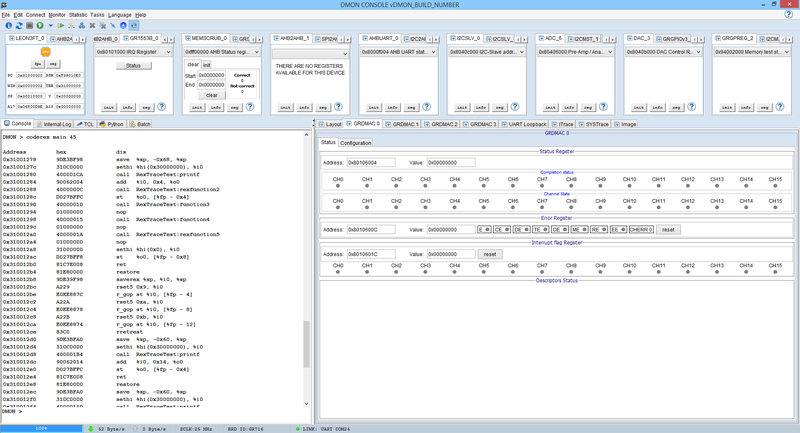
REX Dissembled Instructions
DMON > coderex secondHello

Address         hex               dis
0x31001278      9DE39F98          saverex %sp, %i0, %sp
0x3100127c      A3E830000C7C      rset32	TestContinue_REX_0x31:watchData, %i0
0x31001282      87EA30000C7C      rld32	[TestContinue_REX_0x31:watchData], %o1
0x31001288      83E830000004      rset32	0x30000004, %o0
0x3100128e      E0EE887C          rst %i0, [%fp - 4]
0x31001292      40000181          call TestContinue_REX_0x31:printf
0x31001296      A23F              rset5	0xffffffff, %i0
0x31001298      C4EE807C          rld [%fp - 4], %o1
0x3100129c      E101              rst	%i0, [%o1]
0x3100129e      87E830000028      rset32	0x30000028, %o1
0x310012a4      C0EE8878          rst %o0, [%fp - 8]
0x310012a8      8101              rmov	%o1, %o0
0x310012aa      8508              rmov	%i0, %o1
0x310012ac      4000017A          call TestContinue_REX_0x31:printf
0x310012b0      C0EE8874          rst %o0, [%fp - 12]
0x310012b4      83C0              rretrest
0x310012b6      00009DE3          unimp	0x9de3
0x310012b8      9DE39F98          saverex %sp, %i0, %sp
0x310012bc      A220              rset5	0x0, %i0
0x310012be      E0EE887C          rst %i0, [%fp - 4]
0x310012c2      83E83000004E      rset32	0x3000004E, %o0
0x310012c8      E0EE8878          rst %i0, [%fp - 8]
0x310012cc      40000172          call TestContinue_REX_0x31:printf
0x310012d0      C0EE8874          rst %o0, [%fp - 12]
0x310012d4      7FFFFFE9          call TestContinue_REX_0x31:secondHello
0x310012d8      E0EE8078          rld [%fp - 8], %i0
0x310012dc      83C0              rretrest
The table below shows GR716 REX commands:
| Command | Description |
|---|---|
| rex [en|ill|tr]<cpuID> | Sets the REX mode(enable|illegal|transparent) for active cpu or cpuID if provided |
| coderex [addr]<length> <force> | Disassemble REX instructions in memory. DMON will detect if address is in REX block and disassemble as REX. Force switch will bypass detection and disassemble as REX instruction |
| breakrexs [addr]<cpuID> | Force to set REX Software break point. breaks command will scan if address is in REX block and set REX software break point |
DMA Controller
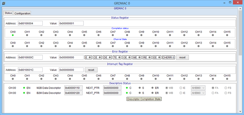
The GR716 microcontroller have 4 separate DMA controller with internal AHB/APB bridge units (GRDMAC). The GRDMAC units described in this section provides a flexible direct memory access controller. The core can perform burst transfers of data between AHB and APB peripherals at aligned or unaligned memory addresses.
One DMA channel per DMA controller is supported. The channel can be configured flexibly by means of two descriptor chains residing in main memory: a Memory to Buffer (M2B) chain and a Buffer to Memory (B2M) chain. Each chain is composed of a linked list of descriptors, where each descriptor specifies an AHB address and the size of the data to read/write, supporting a scatter/gather behavior.
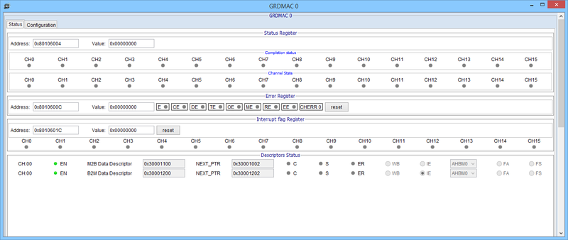
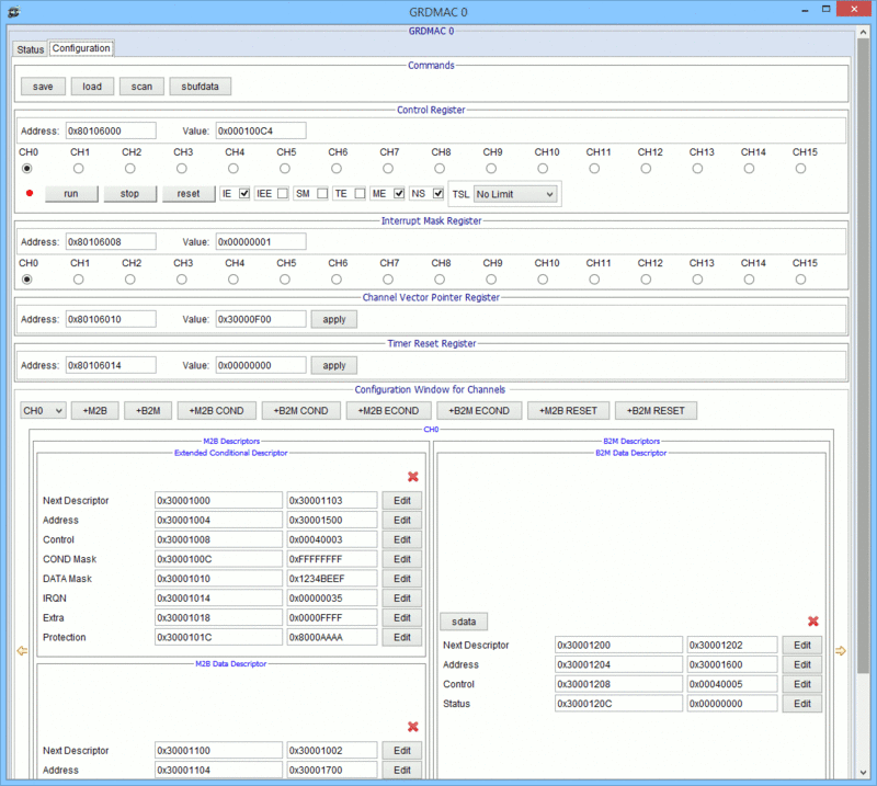
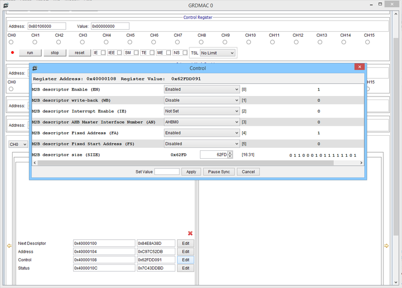
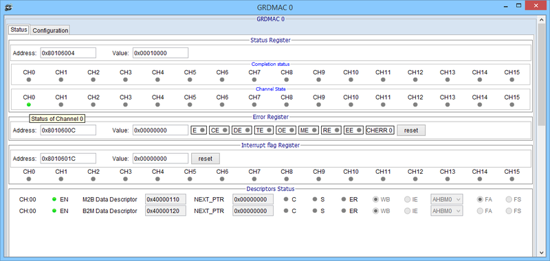
DMON provides a number of specific tabs to allow the user to configure the GRDMAC registers, test DMA transfers, and load/save such test configurations. It is assumed that the user is familiar with the GRDMAC hardware.
GRDMAC status window
GRDMAC configuration window
GRDMAC descriptor configuration
GRDMAC waiting for trigger condition
GRDMAC and Descriptors status after trigger
Available commands for GRDMAC:
| Command | Description |
|---|---|
| grdmac_0 b2m add [data|cond|econd] ch[N][addr] | Create B2M data|conditional|extended conditional descriptors at address for Channel |
| grdmac_0 b2m remove [data|cond|econd] ch[N] [addr] | Remove B2M descriptor at address for Channel |
| grdmac_0 core [en|dis] | Enable(Run) or Disable(Stop) GRDMAC Core |
| grdmac_0 core reset | Reset GRDMAC Core to default values |
| grdmac_0 ctrl ie [en|dis] | Global Interrupt Enable or Disable |
| grdmac_0 ctrl iee [en|dis] | Interrupt Enable or Disable for Errors |
| grdmac_0 ctrl me [en|dis] | Extended Mode Enable or Disable |
| grdmac_0 ctrl ns [en|dis] | No Starve Mode Enable or Disable |
| grdmac_0 ctrl sm [en|dis] | Simplified mode Enable or Disable |
| grdmac_0 ctrl te [en|dis] | Timer Enable or Disable |
| grdmac_0 ech [en|dis][all|ch# ch#+1] | Set Channel/Channels/All Channels Enabled/Disabled |
| grdmac_0 ech [en|dis][ch#-ch#+n] | Set Channel Enabled or Disabled for Range of Channels |
| grdmac_0 eirq [en|dis] | Set Interrupt enable for Errors (IEE) |
| grdmac_0 error reset | Reset Error Register |
| grdmac_0 irq [en|dis] | Set GRDMAC Global Interrupt Enable or Disable (IE) |
| grdmac_0 irq [en|dis][all|ch# ch#+1] | Set Interrupt Mask for Channel/Channels/All Channels and Enable Global IRQ |
| grdmac_0 irq [en|dis][ch#-ch#+n] | Set Interrupt Mask for Range of Channels and Enable Global IRQ |
| grdmac_0 irq reset | Reset Interrupt Flag Register for all channels |
| grdmac_0 load [file] | Load GRDMAC configurations from XML file |
| grdmac_0 m2b add [data|cond|econd] ch[N] [addr] | Create M2B data|conditional|extended conditional descriptors at address for Channel |
| grdmac_0 m2b remove [data|cond|econd] ch[N] [addr] | Remove M2B descriptor at address for Channel |
| grdmac_0 save [file] | Save GRDMAC configuration to XML file |
| grdmac_0 sbufdata | Display Internal Buffer Readout Area |
| grdmac_0 scan | Scan M2B and B2M descriptor linked lists using Channel Vector Pointer |
| grdmac_0 sdata [addr] | Print DMA data after successful B2M Descriptor at address |
| grdmac_0 set cvp [value] | Set Channel Vector Pointer (CVP) |
| grdmac_0 set trv [value] | Set Timer Reset Value (TIMER_RST) |
| grdmac_0 status [offset] | Display GRDMAC core status of All registers or at offset (i.e.0x04) to the screen |
| grdmac_0 tsl [0|32|64|128] | Set Transfer Size limit (TSL) |
DEMO
Basic GRDMAC Custom Configurations:
Use this link if problems with youtube above
Debugging GRDMAC using DMON
Use this link if problems with youtube above
Sample script:
memset write DLRAM_0_START 0x0 // Set Flag to 0 write 0x40000300 0x0 0x400 // Clear memory write 0x30000004 0xcafebabe 0x400 // Set Data to be transferred grdmac_0 core reset // Reset Core grdmac_0 load config.xml // Load GRDMAC and Descriptors configurations. Copy content of thisand save as config.xml grdmac_0 core en // Start the core write DLRAM_0_START 0x1 // Set Flag to 1 to trigger data descriptor grdmac_0 sdata 0x40000120 // Output transferred data
IO Switch Matrix
The I/O switch matrix provides access to several I/O units. When an interface is not activated, its pins automatically become general purpose I/O. After reset, all I/O switch matrix pins are defined as inputs until programmed otherwise.
Configuration and assigning of functions to external I/O is flexible and is controlled by software via a set of registers.
DMON loads in configuration file iomx.config which located in DMON installation directory C:\Program Files (x86)\DMON\Local
User can modify all those configurations or create new custom that will be loaded when DMON starts.
Then, configuration can be applied using "iomx set name" command when DMON started or "-iomx set name" switch command at DMON initialization.
User can autocomplete configuration names using tab after "iomx set" or display all configurations starting with some combination of letters.
| Command | Description |
|---|---|
| iomx set [configName configName ...] | Set IOMX configurations for Device or Array of Devices |
| -iomx set [configName configName ...] | Switch to set IOMX configurations for Device or Array of Devices, when DMON starts |
| iomx setpin [gpioN][val] | Set IOMX GPIO pin to value |
| iomx show <all|configName> | Display all available IOMX configurations or Search by prefix |
| iomx validate | Validate IOMX configurations |
iomx validate sample output:
DMON > iomx validate
GPIO[00]  mem_addr_0
GPIO[01]  mem_addr_1
GPIO[02]  mem_addr_2
GPIO[03]  mem_addr_3
GPIO[04]  mem_addr_4
GPIO[05]  mem_addr_5
GPIO[06]  mem_addr_6
GPIO[07]  mem_addr_7
GPIO[08]  mem_addr_8
GPIO[09]  mem_addr_9
GPIO[10]  mem_addr_10
GPIO[11]  mem_addr_11
GPIO[12]  mem_addr_12
GPIO[13]  mem_addr_13
GPIO[14]  mem_addr_14
GPIO[15]  mem_addr_15
GPIO[16]  mem_addr_16
GPIO[17]  mem_addr_17
GPIO[18]  mem_addr_18
GPIO[19]  ram_csn_0
GPIO[20]  gpio 20
GPIO[21]  gpio 21
GPIO[22]  gpio 22
GPIO[23]  gpio 23
GPIO[24]  gpio 24
GPIO[25]  mem_data_0
GPIO[26]  mem_data_1
GPIO[27]  mem_data_2
GPIO[28]  mem_data_3
GPIO[29]  mem_data_4
GPIO[30]  mem_data_5
GPIO[31]  mem_data_6
GPIO[32]  mem_data_7
GPIO[33]  mem_oen
GPIO[34]  mem_wrn
GPIO[35]  gpio 35
GPIO[36]  gpio 36
GPIO[37]  gpio 37
GPIO[38]  gpio 38
GPIO[39]  gpio 39
GPIO[40]  gpio 40
GPIO[41]  gpio 41
GPIO[42]  gpio 42
GPIO[43]  gpio 43
GPIO[44]  gpio 44
GPIO[45]  gpio 45
GPIO[46]  gpio 46
GPIO[47]  gpio 47
GPIO[48]  gpio 48
GPIO[49]  mem_addr_19
GPIO[50]  mem_addr_20
GPIO[51]  gpio 51
GPIO[52]  gpio 52
GPIO[53]  gpio 53
GPIO[54]  gpio 54
GPIO[55]  gpio 55
GPIO[56]  gpio 56
GPIO[57]  gpio 57
GPIO[58]  gpio 58
GPIO[59]  gpio 59
GPIO[60]  gpio 60
GPIO[61]  gpio 61
GPIO[62]  gpio 62
GPIO[63]  gpio 63
iomx validate sample output with duplicated pin configurations:
DMON > iomx validate
GPIO[00]  mem_addr_0
GPIO[01]  mem_addr_1
GPIO[02]  mem_addr_2
GPIO[03]  mem_addr_3
GPIO[04]  mem_addr_4
GPIO[05]  mem_addr_5
GPIO[06]  mem_addr_6
GPIO[07]  mem_addr_7
GPIO[08]  mem_addr_8
GPIO[09]  mem_addr_9
GPIO[10]  mem_addr_10
GPIO[11]  mem_addr_11
GPIO[12]  mem_addr_12
GPIO[13]  can_tx_0
GPIO[14]  can_rx_0
GPIO[15]  can_en_0
GPIO[16]  mem_addr_16
GPIO[17]  mem_addr_17
GPIO[18]  mem_addr_18
GPIO[19]  ram_csn_0
GPIO[20]  gpio 20
GPIO[21]  gpio 21
GPIO[22]  gpio 22
GPIO[23]  gpio 23
GPIO[24]  gpio 24
GPIO[25]  mem_data_0
GPIO[26]  mem_data_1
GPIO[27]  mem_data_2
GPIO[28]  mem_data_3
GPIO[29]  mem_data_4
GPIO[30]  mem_data_5
GPIO[31]  mem_data_6
GPIO[32]  mem_data_7
GPIO[33]  mem_oen
GPIO[34]  mem_wrn
GPIO[35]  gpio 35
GPIO[36]  gpio 36
GPIO[37]  can_tx_0 Already mapped
GPIO[38]  can_rx_0 Already mapped
GPIO[39]  can_en_0 Already mapped
GPIO[40]  gpio 40
GPIO[41]  gpio 41
GPIO[42]  gpio 42
GPIO[43]  gpio 43
GPIO[44]  gpio 44
GPIO[45]  gpio 45
GPIO[46]  gpio 46
GPIO[47]  gpio 47
GPIO[48]  gpio 48
GPIO[49]  mem_addr_19
GPIO[50]  mem_addr_20
GPIO[51]  gpio 51
GPIO[52]  gpio 52
GPIO[53]  gpio 53
GPIO[54]  gpio 54
GPIO[55]  gpio 55
GPIO[56]  gpio 56
GPIO[57]  gpio 57
GPIO[58]  gpio 58
GPIO[59]  gpio 59
GPIO[60]  gpio 60
GPIO[61]  gpio 61
GPIO[62]  gpio 62
GPIO[63]  gpio 63
Memory Protection
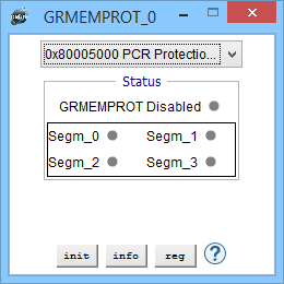
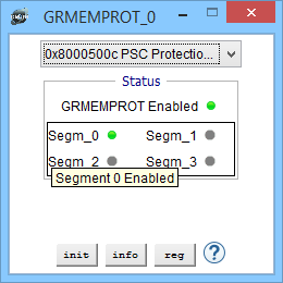
The GR716 microcontroller has 2 separate AMBA memory protection units (MEMPROT). The MEMPROT units have the capability to detect and protect memory areas from write accesses. The first memory protection unit (MEMPROT0) is connected to Main AHB bus and the second memory protection unit (MEMPROT1) is connected to the DMA AMBA bus. Each memory protection unit has a unique address for configuration and status. The control and status registers for the memory protection units are located on APB bus in the address range 0x80005000 to 0x80005FFF 0x8010A000 to 0x8010AFFF.
DMON provides the commands below to configure memory protection.
| Command | Description |
|---|---|
| mprot reg | Show GRMEMPRO registers |
| mprot set [n][saddr][eaddr][none|all|g0-g15..] | Protect area [seg num][s address][e address][none|all or array of g0-g15] |
Memory Protection Device View
Memory Protection Device View (enabled)
Clock Gating options
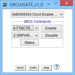
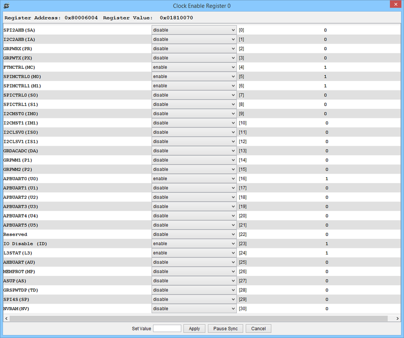
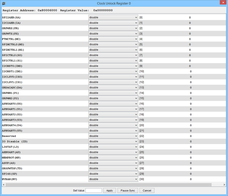
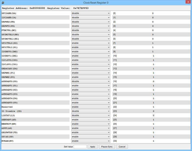
The GR716 microcontroller have 2 separate clock gating units. Each clock gating unit will control its own clock domains and have a unique AMBA address.
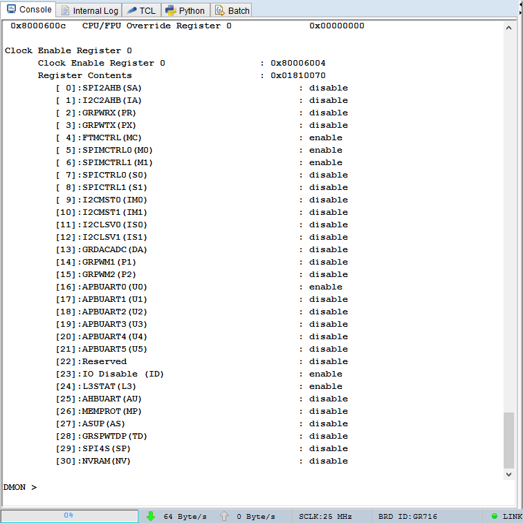
The clock gating units provide a means to save power by disabling the clock to unused functional blocks. These cores provide a mechanism to automatically disable the clock to LEON processors in power-down mode, and optionally also to disable the clock for shared floating-point units. The cores also provide a mechanism to reset, enable clock and disable clocks for most functional blocks.
| Command | Description |
|---|---|
| grcg [enable|disable][all|bit..bitN] | Enable|Disable all, single bit or array of bits for GRCLKGATE_0 |
| -grcg [enable|disable][all|bit..bitN] | Switch to Enable|Disable all, single bit or array of bits for GRCLKGATE_0 or -grcg_1 for GRCLKGATE_1, at DMON start up |
| grcg reg | Show register values for GRCLKGATE_0 |
Commands
The table below is a summary of commands specific to the GR716.
| Command | Description |
|---|---|
| breakrexs [addr]<cpuID> | Force to set REX Software break point. breaks command will scan if address is in REX block and set REX software break point |
| coderex [addr]<length> <force> | Disassemble REX instructions in memory. DMON will detect if address is in REX block and disassemble as REX. Force switch will bypass detection and disassemble as REX instruction |
| dlram edac [enable|disable] | Enable|Disable EDAC |
| dlram scrub [enable|disable] | Enable|Disable Scruber |
| gpio pulse status | Show Pulse register for GRGPIO |
| gradcdac config | Display status information for the GRADCDAC core |
| grcan [enable|disable] | Enable|Disable the GRCAN receiver |
| grcan reset | Resets the GRCAN receiver |
| grcan status | Show register values for GRCAN |
| grcg [enable|disable][all|bit..bitN] | Enable|Disable all, single bit or array of bits for GRCLKGATE_0 |
| grcg reg | Show register values for GRCLKGATE_0 |
| grdmac_0 b2m add [data|cond|econd] ch[N][addr] | Create B2M data|conditional|extended conditional descriptors at address for Channel |
| grdmac_0 b2m remove [data|cond|econd] ch[N] [addr] | Remove B2M descriptor at address for Channel |
| grdmac_0 core [en|dis] | Enable(Run) or Disable(Stop) GRDMAC Core |
| grdmac_0 core reset | Reset GRDMAC Core to default values |
| grdmac_0 ctrl ie [en|dis] | Global Interrupt Enable or Disable |
| grdmac_0 ctrl iee [en|dis] | Interrupt Enable or Disable for Errors |
| grdmac_0 ctrl me [en|dis] | Extended Mode Enable or Disable |
| grdmac_0 ctrl ns [en|dis] | No Starve Mode Enable or Disable |
| grdmac_0 ctrl sm [en|dis] | Simplified mode Enable or Disable |
| grdmac_0 ctrl te [en|dis] | Timer Enable or Disable |
| grdmac_0 ech [en|dis][all|ch# ch#+1] | Set Channel/Channels/All Channels Enabled/Disabled |
| grdmac_0 ech [en|dis][ch#-ch#+n] | Set Channel Enabled or Disabled for Range of Channels |
| grdmac_0 eirq [en|dis] | Set Interrupt enable for Errors (IEE) |
| grdmac_0 error reset | Reset Error Register |
| grdmac_0 irq [en|dis] | Set GRDMAC Global Interrupt Enable or Disable (IE) |
| grdmac_0 irq [en|dis][all|ch# ch#+1] | Set Interrupt Mask for Channel/Channels/All Channels and Enable Global IRQ |
| grdmac_0 irq [en|dis][ch#-ch#+n] | Set Interrupt Mask for Range of Channels and Enable Global IRQ |
| grdmac_0 irq reset | Reset Interrupt Flag Register for all channels |
| grdmac_0 load [file] | Load GRDMAC configurations from XML file |
| grdmac_0 m2b add [data|cond|econd] ch[N] [addr] | Create M2B data|conditional|extended conditional descriptors at address for Channel |
| grdmac_0 m2b remove [data|cond|econd] ch[N] [addr] | Remove M2B descriptor at address for Channel |
| grdmac_0 save [file] | Save GRDMAC configuration to XML file |
| grdmac_0 sbufdata | Display Internal Buffer Readout Area |
| grdmac_0 scan | Scan M2B and B2M descriptor linked lists using Channel Vector Pointer |
| grdmac_0 sdata [addr] | Print DMA data after successful B2M Descriptor at address |
| grdmac_0 set cvp [value] | Set Channel Vector Pointer (CVP) |
| grdmac_0 set trv [value] | Set Timer Reset Value (TIMER_RST) |
| grdmac_0 status [offset] | Display GRDMAC core status of All registers or at offset (i.e.0x04) to the screen |
| grdmac_0 tsl [0|32|64|128] | Set Transfer Size limit (TSL) |
| grpwm <dev#> enable|disable | Enable or Disable the GRPWM core |
| grpwm <dev#> status | Display status information for the GRPWM core |
| grpwrx [enable|disable] | Enable|Disable the GRPWRX reciever |
| grpwrx dma [enable|disable] | GRPWRX dma Enable|Disable |
| grpwrx reset | Resets the GRPWRX reciever |
| grpwrx status | Show register values for GRPWRX |
| grpwtx [enable|disable] | Enable|Disable the GRPWTX reciever |
| grpwtx dma [enable|disable] | GRPWTX DMA Enable|Disable |
| grpwtx reset | Resets the GRPWTX Transmitter |
| grpwtx status | Show register values for GRPWTX |
| i2c2ahb enable|disable | Enable or Disable the I2C2AHB core |
| i2c2ahb irq enable|disable | Display status information for the I2C2AHB core |
| i2c2ahb status | Display status information for the I2C2AHB core |
| ilram edac [enable|disable] | Enable|Disable EDAC |
| ilram scrub [enable|disable] | Enable|Disable Scruber |
| iomx set [configName configName ...] | Set IOMX configurations for Device or Array of Devices |
| iomx setpin [gpioN][val] | Set IOMX GPIO pin to value |
| iomx show <all|configName> | Display all available IOMX configurations or Search by prefix |
| iomx validate | Validate IOMX configurations |
| mprot reg | Show GRMEMPRO registers |
| mprot set [n][saddr][eaddr][none|all|g0-g15..] | Protect area [seg num][s address][e address][none|all or array of g0-g15] |
| rex [en|ill|tr]<cpuID> | Sets the REX mode(enable|illegal|transparent) for active cpu or cpuID if provided |
| spi2ahb enable|disable | Enable or Disable the SPI2AHB core |
| spi2ahb irq enable|disable | Enable or disable interrupts for SPI2AHB core |
| spi2ahb status | Display status information for the SPI2AHB core |
| spislave status | Show registers values for SPI4SPACE |
| spislave reset | Reset SPI4SPACE device |
| spim edac <enabled|disable> | Enable or Disable EDAC in SPIMCTRL |
| spwtdp status | Display status information for the SPWTDP core |
PROM Builder
DMON PROM Builder Introduction
DMON Prom Builder can be used to configure basic prom settings, create prom file and use DMON commands to load to the target flash. This feature is available in DMON 2.1.0.0 version.
Prom Builder Features:
- Save configurations to the property file
- Load saved configurations
- DMON is displaying current target memory settings for mkprom2 memory switches
- Easy to set basic prom configurations
- Prom Builder is creating make file, which can be examined and used on its own through DMON "buildprom" command or called directly from CLI with make utility
- Prom Builder is calling DMON flash commands after prom file was created to erase flash, check if blank, load prom file to target flash and start program on the board
DMON provides two prom configuration files for E698PM. They located in DMON install directory at DMON\Files\PROM_PM_CONFIG initially and copied to DMON user folder C:\Users\UserName\DMON\PromConfig when Prom Builder is started for the first time. 698PM_RAM_PROM.properties file has configurations that can be used to produce prom file to use RAM only as it does not initialize DDR2 RAM. 698PM_DDR_PROM.properties file has configurations to produce prom file to use DDR2 RAM on E698PM. Sample bdinit.c file is located in DMON\Files\PROM_PM_CONFIG directory. This file has to be compiled and put in the same directory where make file will be stored. bdinit.c can be copied from bdinit.c too.
Please follow the tutorials below. The sample program for E698PM used in tutorials can be found here.
DMON Prom Builder can be called from DMON menu => Tasks => Prom Builder.
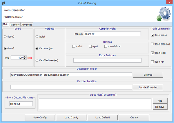
DMON Prom Builder Main View:
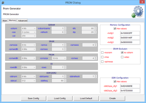
DMON Prom Builder Memory View:
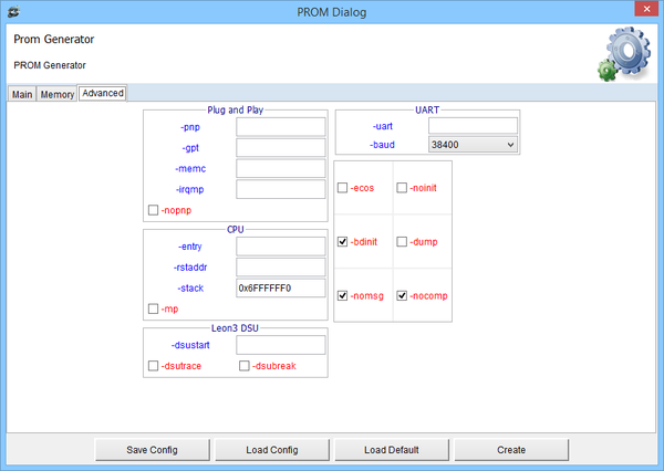
DMON Prom Builder Advanced View:
DMON Commands
| Command | Description |
|---|---|
| buildprom <cmderase,cmdblank,cmdload,cmdrun> mkf | Create prom by calling mkf in make utility. Pass flash commands as parameters. buildprom cmderase cmdload cmdrun my_make_file |
DMON PROM Builder Tutorials
Creating sample prom file using RAM only:
Use this link if problems with youtube above
Creating prom file to be used with DDR2 RAM:
Use this link if problems with youtube above
Building PROM file using make:
Use this link if problems with youtube above
Creating prom file calling directly mkprom2 from CLI:
